
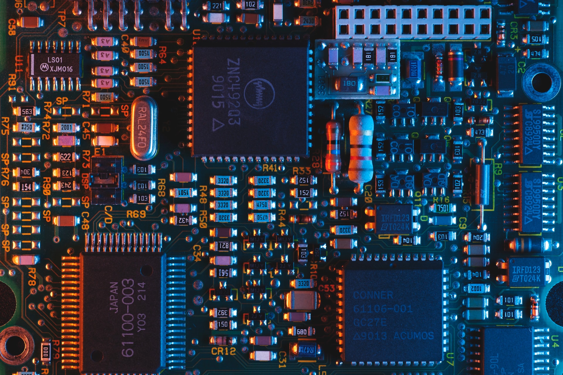
Based on a recent study conducted by Research and Markets, the global printed circuit board market is expected to grow to $75.72 billion come 2025. With a compound annual growth rate of 4.12%, the industry’s boom in recent years is mainly attributed to the continuous development of and ever-growing need for consumer electronics. This is why it is important to point out that field, and specifically PCBs are mechanical too, not just electrical.
If mechanical engineers think that this speedily growing sector is none of their concern, then they have to think again. As we previously highlighted here on the blog, one of the duties of mechanical engineers — especially those working in the electrical field — is to assist in the design and manufacturing of electrical products. Since PCBs serve as the “brain” and backbone of most electronic devices today, it only makes sense for mechanical engineers to develop a certain level of interest in them.
In addition to this, it is also important for many mechanical engineers to realize that PCBs are mechanical, as well as being electrical. In fact, one can even go as far as saying that PCBs are a great example of mechatronics, which combine electrical and mechanical design practices. But if you are still not convinced, then here some of the ways PCBs are indeed mechanical.
Library Development
PCBs are made with two different tools: the electronic CAD (ECAD) for the footprint and the mechanical CAD (MCAD) for the components embedded on them. Back then engineers used these two tools separately to create a mechanical design workflow that can be integrated into an electrical design application. Such a setup was met with a lot of challenges. For one, it increased the likelihood of inaccurate design transfer, which drastically increases the number of design spins. In some cases, poor electromechanical co-design processes can even result in missed deadlines and skyrocketing costs, all due to how time-consuming it can be to fix design mistakes.
Thankfully, we now have ECAD-MCAD collaboration tools. Modern types of PCB design software are now capable of creating 3D components in a footprint library — making the design process faster than ever. Having both ECAD and MCAD on one platform has also helped designers accurately analyze mechanical clearances, leading to better-built circuitry. Applications like these also allow for quicker, easier, and more accurate transfer of data from one tool to another. In just a few clicks, electrical and mechanical engineers working on a PCB can now import design content and have access to board outline, component placements, and mounting holes.
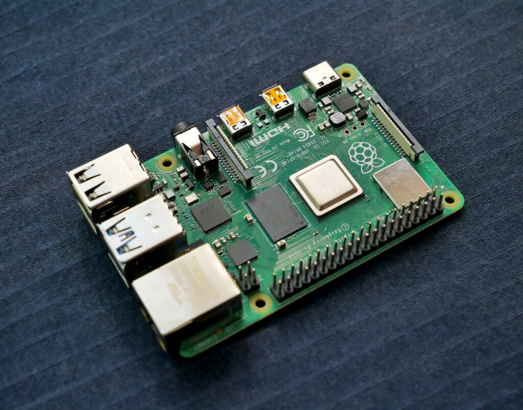
Board Shape
In most cases today, the look of a product comes from the marketing department. The same rule applies to printed circuit boards. In spite of the fact that PCBs are mechanical in nature, their design is usually influenced by the marketing department, and it is the mechanical team’s job to bring the former’s ideas into a 3D representation. This is the reason why mechanical teams have to have practical knowledge about PCBs.
Now that electronic devices are coming in all sorts of shapes and sizes, mechanical teams must learn how to do away with square or rectangular boards. If in the past, it was the final product of the PCB layout that determines the design of the enclosure, these days, it’s actually the other way around. Developers of modern MCAD tools are well-aware of this reality, which is why they now allow for products that are anything but square. Nowadays, a lot of board shapes can be imported from MCAD tools based on the dimensions of the enclosures.
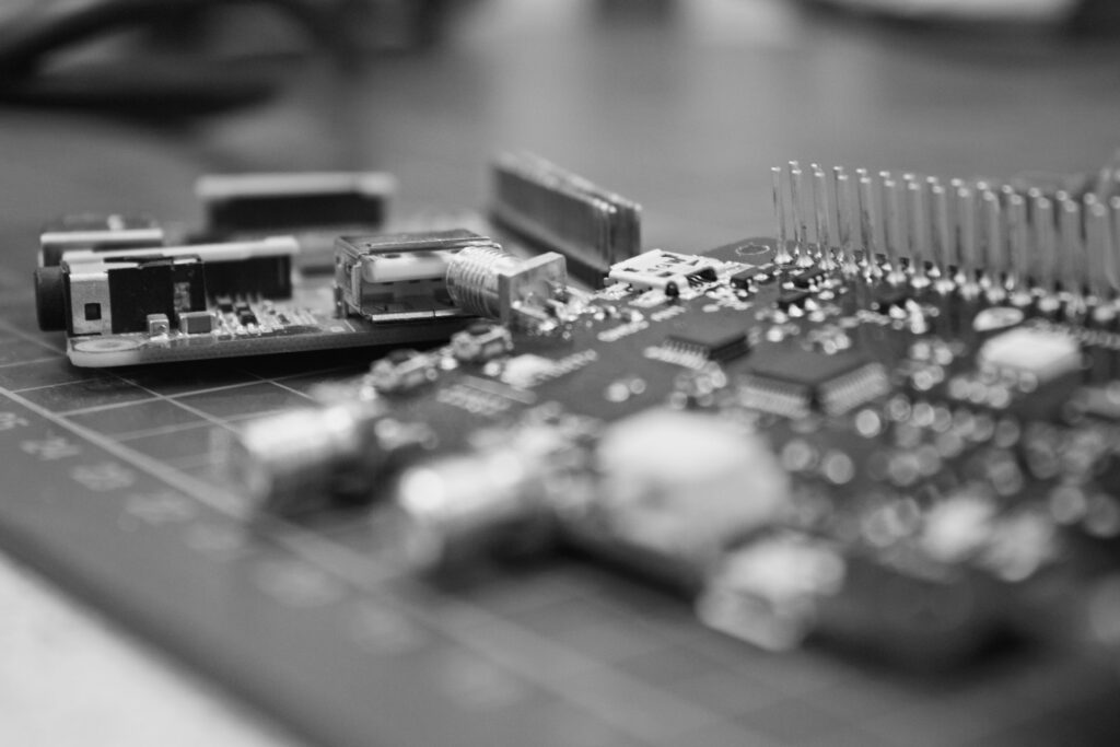
Component Placement
Aside from board shape, component placement is also turning out to be another area that is becoming more and more driven by mechanical design. Thanks to collaborative PCB software programs, it is now commonplace to pass the board and its components between ECAD and MCAD tools. This allows engineers to check the key locations of the components that the end-user will press or connect through a cable.
Collaboration also enables engineers to sort and determine the electrical and mechanical aspects of component placement before the actual routing occurs. This step is undoubtedly an example of mechatronic design in action since it considers both the electrical and mechanical needs of PCBs all at once. Through this, engineers can prevent fitment conflicts, avoid missing high-profile components, and keep enclosures from being excessively prevalent in the design before they proceed with PCB fabrication and mass production.
Thank you very much for being here – we appreciate you taking the time to read our content. Do you have any experience with PCBs? Feel free to leave a comment down below – we would love to hear from you! And sign up to our newsletter for more of the same!
You can also follow us on LinkedIn, Facebook, Twitter, and Instagram so you can stay up to date. If you would like to learn more about mechanical engineering you can find more articles on our blog.

1 thought on “Why PCBs Are Mechanical Components”
There are two directions that have high requirements for PCB design: one is the high-power PCB, such as the power electronics field; the other is the high-speed PCB, such as the signal and radio frequency fields. In these two areas, in addition to connecting wires, there are many advanced skills: how large the wire diameter is (is the current capacity enough?), how to route the wires (90 degrees or 45 degrees), and the relationship between wires (parasitic inductance) , How big is the parasitic capacitance), the distance between the line and the line (is enough withstand voltage?), the interaction of the generated magnetic field/electric field, etc.), how to layout the devices, how to distribute the power supply system… It’s so much!